| houkime | i am ill to a half-dead state. A flu. But still ned to do sth not really requiring much brain, so made an fp, a sch and preliminary placement for the new stylus proximity sensor. | 00:38 |
|---|---|---|
| houkime | for exact placement tomorrow will do an fp of a projection of a stylus on a LOWER and exactly place it. | 00:39 |
| houkime | also an fp for a artistic orifice sensor looks through. | 00:39 |
| houkime | need to shove myself somewhere and try to survive the night while oozing with body fluids. | 00:41 |
| Oksana | houkime: Hope you get better soon! Hot tea, honey, ginger, oranges, or whatever else can help. Flu can be deadly, so take care. | 02:43 |
| sixwheeledbeast | It's going round. I still have an ear infection 2 months after I got rid of mine. | 08:45 |
| houkime | made and placed a stylus projection, and also calculated the orifice and made an fp for it | 09:03 |
| houkime | will need to play a bit with 3d tetris problem of a tall modemso that it doesn't collide with aux components of the sensor. | 09:05 |
| houkime | but now it is again time to return to a wooden log state and recuperate. | 09:06 |
| houkime | the orifice itself resulted to be quite big - 2.1 mm radius. If LED is in this radius it doesn'r really need an orifice protrusion for itself - it won't really increase gain at all. | 09:08 |
| Joerg-Neo900 | >><n00buser> Joerg-Neo900, so if you get enough funding you will be able to finish the project?<< actually not, since availability of mission critical parts dwindled over time and the whole concept isn't competitive anymore | 12:58 |
| Joerg-Neo900 | >>2.1 mm radius<< seems prohibitively large for anything except core chipset stuff | 13:01 |
| Joerg-Neo900 | a 25mm^2 bite out of our available real estate isn't tolerable for this | 13:02 |
| Joerg-Neo900 | I'm also still concerned my idea didn't make it to the public sense: the led sits on S2 and shines DOWNward through a dedicated hole in S2-S1 PCB. When stylus gets inserted, this hole gates "hermetically sealed" by stylus so no light may escape from LED and its hole to anywhere. Same applies likewise for light sensor sensing refelxions of light on wall of stylus bay as long as no stylus inserted and hermetically sealing *both* holes | 13:07 |
| Joerg-Neo900 | It totally evades me where a 2.1mm radius comes in here | 13:07 |
| Joerg-Neo900 | both LED and sensor need max 2mm DIAMETER holes | 13:08 |
| Joerg-Neo900 | rather less | 13:08 |
| Joerg-Neo900 | anyway there must not be any "bypass" path from LED to sensor by them using same hole in PCB | 13:09 |
| houkime | The mechanism of detection has changed a bit. I will just explain calibration procedure so it is clear. LED and sensor sit together and look downwards through a hole or holes. First, there is a stylus behind a hole. One plays with number of pulses per measurement and LED current so that number of ADC counts ("reflection yield") becomes big enough. this is now our "yield with stylus". | 13:29 |
| houkime | then the stylus is removed | 13:29 |
| houkime | and the measurement is performed again, without changing number of pulses and current | 13:30 |
| houkime | and you obtain the second number, "yield with no stylus" | 13:30 |
| houkime | yield with no stylus should be discernable from yield with stylus, (probably it is lower than with stylus) if adc count with stylus is high enough to distinguish them. | 13:32 |
| houkime | then one writes stylus detection thresholds into a chip via i2c so that it can generate interrupts. | 13:35 |
| houkime | and finally one sets up a timer inside the chip so it performs measurements automatically. | 13:36 |
| houkime | Joerg-Neo900, is it clear now? | 13:36 |
| houkime | the scheme with separate holes and stylus blocking path is also possible, one just needs to put LED a little be farther away. | 14:00 |
| houkime | i doubt there is space for that though, everything is kinda tight. Also if LED is farther the yield is lower. | 14:01 |
| houkime | though this one is arguable since the maximum yield can be lower without detection reliability issues with separate holes. | 14:02 |
| houkime | We want to cut off picking up reflections from LOWER itself to maximize detection efficiency. This is why hole against the sensor is kinda large - it is based on the angular sensitivity distribution and the distance between boards (chip has clear package) | 14:06 |
| houkime | so in some sense sensor doesn't even "see" LOWER. | 14:07 |
| Joerg-Neo900 | there is no way to pick up reflexions from LOWER since sensors sit on S2 looking downwards through the PCB 0.0mm away | 14:09 |
| houkime | Joerg-Neo900, it is not 0.0 mm away. It is 2.5 mm away. the package is clear plastic/ | 14:10 |
| Joerg-Neo900 | you still seem to place sensors on S3 | 14:10 |
| Joerg-Neo900 | no | 14:10 |
| Joerg-Neo900 | no idea what sensors you use and where you place them. We planned for sensor sitting on one PCB and looking downwards through a hole in that very PCB | 14:11 |
| Joerg-Neo900 | those sensors are not supposed to pick up reflexions from the PCB they are mounted to | 14:12 |
| houkime | i agree that that would be ideal, but i haven't found such a part. And TMDxx sensor that was in original sch is not such a part either. Unless in the clear package one can sense from the other side of the die. | 14:14 |
| Joerg-Neo900 | I'm sorry I didn't design (prolly neither reviewed) details of that sensor. The concept was clear between all who were involved. Maybe check if that part could get soldered top down | 14:16 |
| Joerg-Neo900 | toldya optical proximity sensors were a PITA and a source-ability nightmare all the time, all seens several changes of parts | 14:17 |
| Joerg-Neo900 | you find a nice part, 2 weeks later it's EOL# | 14:18 |
| Joerg-Neo900 | :-/ | 14:18 |
| Joerg-Neo900 | you seatrch for a compatible new part, find one, 3 weeks later EOL that as well | 14:19 |
| Joerg-Neo900 | sorry I'm not in that business anymore | 14:19 |
| Joerg-Neo900 | it's a pity but we have to accept large parts of Neo900 design became obsolete and worth sh*t | 14:20 |
| Joerg-Neo900 | lesson learned: even while you design for 3 alternative part sources maybde even with multi purpose footprint, you must not take longer than a 6 months between schematics design start and start of production or at least sourcing | 14:22 |
| Joerg-Neo900 | industry became a bitch | 14:22 |
| Joerg-Neo900 | all hail to TI for still selling OMAP3 | 14:23 |
| Joerg-Neo900 | how much longer? | 14:23 |
| Joerg-Neo900 | when you want to place sensor on S3, you not only use the real estate of the sensor and LED on S3 but also TWO times 25mm^2 on S1 and S2. Complete nogo | 14:25 |
| Joerg-Neo900 | nuke that shit, feature <<< cost | 14:26 |
| houkime | Joerg-Neo900, what is the clearance between stylus and LOWER? | 14:29 |
| Joerg-Neo900 | zero | 14:30 |
| Joerg-Neo900 | remember my explanation of "hermetically sealed" holes with stylus inserted? | 14:31 |
| Joerg-Neo900 | lends itself excellently to a capacitive sensor on PCB instead | 14:31 |
| houkime | checked TMDxx series once again - no, obviously can't be mounted top-down. | 14:35 |
| houkime | ok, nuking then. | 14:35 |
| houkime | chances of finding a good part for this are near zero and if if one finds it - EOL is a problem indeed. | 14:36 |
| houkime | the optical lid sensor on BOB is sourced from N900 or it also needs reviewing? | 14:38 |
| Joerg-Neo900 | the latter | 14:39 |
| Joerg-Neo900 | also already seen 2 reworks iirc | 14:39 |
| Joerg-Neo900 | luckily facing up | 14:40 |
| houkime | there might be no place there for SI115x-like sensor, so integrated expensive stuff might be the only way in this case. Need to check. | 14:40 |
| Joerg-Neo900 | alternative: vintage component sourcing | 15:10 |
| Joerg-Neo900 | there might be still a few 1000 of those Osram SFH(?) proximity sensorsa available out there | 15:10 |
| houkime | SI115x seems to marginally fit. might work. | 15:52 |
| houkime | however i am a bit worried that while nonzero, availability of SI115x is not amazing. Might phase out at some point. | 15:53 |
| houkime | clearly not the most popular component family in the world. | 15:54 |
| houkime | i don't know prices on vintage components. Might be even more expensive than modern stuff. | 16:05 |
| houkime | need to review BOB connectors before anything though. Cause right now situation on the BOB is quite nasty. | 18:19 |
| houkime | and connectors are the primary reason for this. | 18:20 |
| houkime | interesting question is what is the allowed range of stacking heights. Cause there are no things on BOB that need to be in direct contact with the case. | 18:39 |
| houkime | the most sensitive to this is probably the hall sensor. | 18:40 |
| houkime | and if one can reduce stacking height, then one can use connectors with smaller fps | 18:42 |
| houkime | sd card is also a bit sensitive since you need to be able to insert stuff into it. | 18:43 |
| Joerg-Neo900 | you can't reduce stacking height much | 18:44 |
| Joerg-Neo900 | hackerbuss conneector is also sensitive to geometry | 18:45 |
| Joerg-Neo900 | see hb whitepaper | 18:45 |
| houkime | it might be possible to make hb connector not hanging from below but be a normal connector instead and simultaneously reduce stacking height. | 18:48 |
| houkime | so that effective interface height remains the same | 18:48 |
| houkime | but sd card is unlikely to tolerate such a radical thing. | 18:49 |
| houkime | need to check. | 18:50 |
| houkime | molex 52465 series offers a funny solution to connector problems | 21:01 |
| houkime | these parts's placement is quite inaccurate and 2 of them is not an option | 21:01 |
| houkime | but if one chooses 40 pin variant it's physical length is 17.6 mm | 21:02 |
| houkime | and it marginally fits on BOB horizontally | 21:02 |
| houkime | it is possible because pitch is 0.8 mm and stacking height is 4.5 mm | 21:03 |
| houkime | not to mention that i can place it diagonally like i already do with DF9 | 21:10 |
| houkime | so that it is not really that marginal anymore | 21:10 |
| houkime | Joerg-Neo900, what is exact reason for board guide and high accuracy placement requirement? | 21:12 |
| DocScrutinizer51 | bob nees support by 3 points that form a triangle of max possible area | 21:12 |
| DocScrutinizer51 | BoB has nasty tolerances | 21:13 |
| houkime | is it possible to provide support additionally without connectors? Like with a pure mechanical part? | 21:13 |
| DocScrutinizer51 | sure | 21:13 |
| houkime | So as i understand, connector placement error will translate into BoB placement error, and BoB placement requirements are tight. | 21:16 |
| houkime | especially so that i expanded it a little based on 3D scan data. | 21:16 |
| houkime | at the same time, if 40 pin connector is placed diagonally i can shrink Bob back and maybe even more than original | 21:18 |
| houkime | thus alleviating needed strictness of BoB position | 21:18 |
| DocScrutinizer51 | yhere are pogopin guides that need exact position | 21:19 |
| houkime | DocScrutinizer51, what is the tolerance on those? | 21:23 |
| houkime | they are not soldered or anything, they just need to touch firmly enough, right? | 21:24 |
| houkime | *pogos touch contacts on LOWER | 21:25 |
| DocScrutinizer51 | they need to get guided to their position. see hb.pdf | 21:25 |
| houkime | DocScrutinizer51, yea, i know, the cutouts. How strict those need to be not to prevent contact? | 21:26 |
| DocScrutinizer51 | please see hb.pdf | 21:26 |
| houkime | DocScrutinizer51, hb.pdf has a page 9 on pogo pins and it doesn't say anything about tolerances on pogo pins. | 21:31 |
| houkime | neither does the exact placement drawing | 21:32 |
| DocScrutinizer51 | but it shows the requirementgs | 21:32 |
| houkime | ok, the guides (radius 0.9) are quite tight around a pin which has a radius of around 0.8. | 21:37 |
| houkime | however guides and user board are mechanically coupled via connector | 21:38 |
| houkime | so bob placement error won't produce pogos failing to go into guides | 21:38 |
| houkime | what it will produce is some error in finding the contact on the LOWER | 21:39 |
| DocScrutinizer51 | igh, please reread, the pogo pins are longer than the HB connector | 21:39 |
| DocScrutinizer51 | and yes, they need to find contacts on LOWER | 21:40 |
| houkime | DocScrutinizer51, i know that they a longer. How it is connected to what i have said? | 21:40 |
| DocScrutinizer51 | sorry I don't have the capacity to re-iterate the complee design process | 21:41 |
| DocScrutinizer51 | which took well over a week or two with wpwrak | 21:42 |
| DocScrutinizer51 | wek didn't choose B2B spacing or BoB shape lightly since we were bored | 21:43 |
| DocScrutinizer51 | it took days to find the B2B conns | 21:43 |
| houkime | ok, will do it myself then. The design was flawed mostly because you didn't cosider USB connector on the LOWER whiich prevents connector placement as you originally designed. | 21:43 |
| DocScrutinizer51 | possible | 21:44 |
| houkime | and from there everything crumbled unfortunately. | 21:44 |
| DocScrutinizer51 | USB is on S2, BoB connects to S1 | 21:46 |
| DocScrutinizer51 | USB has TH fixtures | 21:46 |
| DocScrutinizer51 | those should be rather short so if they interfere with anything on S1, we could do partial PCB stack cutout | 21:47 |
| DocScrutinizer51 | I'd be surprised if wpwrak AND I both didn't notice a collision to USB | 21:50 |
| Joerg-Neo900 | partial PCB stack cutout == basically a kingsize blind via | 21:54 |
| Joerg-Neo900 | please ölet me know if that keeps your concern about USB BoB-B2Bconn colision intact or voided it | 21:56 |
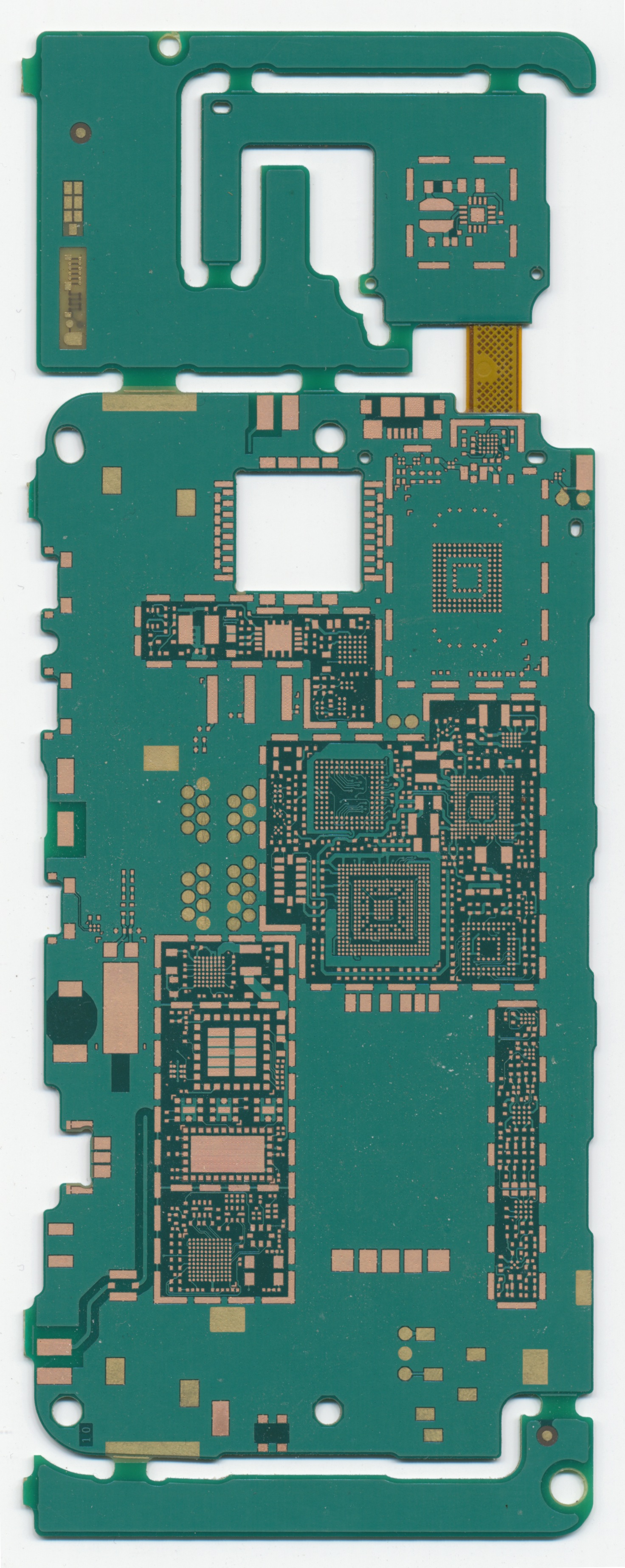
| houkime | it is not on S2. It is on S1. Look at this bareboard shot http://neo900.org/stuff/Gallery-N900-exploded/platine_02.jpeg | 21:58 |
| Joerg-Neo900 | *if* B2Bconn for BoB has guide pins, those can get shortened do not impair USB | 21:59 |
| Joerg-Neo900 | I looked at the board itself | 21:59 |
| Joerg-Neo900 | and damn, you're right | 21:59 |
| Joerg-Neo900 | :-S | 22:00 |
| Joerg-Neo900 | however BoB and USB oevrlap only a 1mm plus contact courtyard | 22:01 |
| Joerg-Neo900 | given total size og BoB I can't imagine how this could cause an unsurnountable collision | 22:02 |
| houkime | directly physically maybe, but the thing is one needs to place an fp for a connector on LOWER also and maintain clearances. this leads to around 4 mm of excluded space | 22:03 |
| houkime | if i am not terribly wrong (did calculations a year ago, and not one time. Could have missed sth though) | 22:04 |
| houkime | 4 mm was enough to screw things up entirely. I ned to place things in a very bizarre manner. | 22:09 |
| houkime | and it can kinda work, but seems very unreliable and marginal. | 22:10 |
| houkime | that said, i will recheck everything once again | 22:12 |
| DocScrutinizer51 | feel free to design any more reliable solution, incl embedded FPC PCB like original | 22:12 |
| DocScrutinizer51 | we didn't find any, that's why it took so long | 22:12 |
| houkime | btw it seems like usb connector fp on neo900 is around 1 mm longer than it is on original RX-51 | 22:31 |
| Joerg-Neo900 | I'm not involved in footprints | 22:31 |
| Joerg-Neo900 | alas during design phase we had no layouter contributing their thoughts | 22:32 |
| Joerg-Neo900 | I repeatedly asked urgently for some layouter contributing fp ahead of layout time since the fp are completely unrelated to schematics | 22:34 |
| Joerg-Neo900 | since this didn't happen, we had to rely on fp in datasheets if we ever pondered about them | 22:34 |
| Joerg-Neo900 | the argument we heard always been "you might change one or two components during schematics design so it doesn't make sense to create fp right now" | 22:36 |
| Joerg-Neo900 | other layouters told us they create footprints on the fly while routing the layout | 22:37 |
| Joerg-Neo900 | sorry I really don't care anymore | 22:37 |
| Joerg-Neo900 | I'm still more than busy cleaning up the broken pieces of everything | 22:38 |
| Joerg-Neo900 | incl own health | 22:38 |
| houkime | Don't be so negative) 10+ of my friends are in jail now and i don't know what will be tomorrow, but i still want to do stuff and learn. | 22:42 |
Generated by irclog2html.py 2.17.0 by Marius Gedminas - find it at https://mg.pov.lt/irclog2html/!